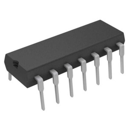
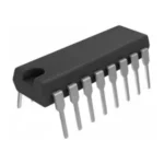
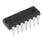
74HC74 – 7474 ( Dual D-type flip-flop with set and reset )
Original price was: 24.37 EGP.21.90 EGPCurrent price is: 21.90 EGP.
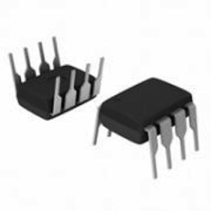
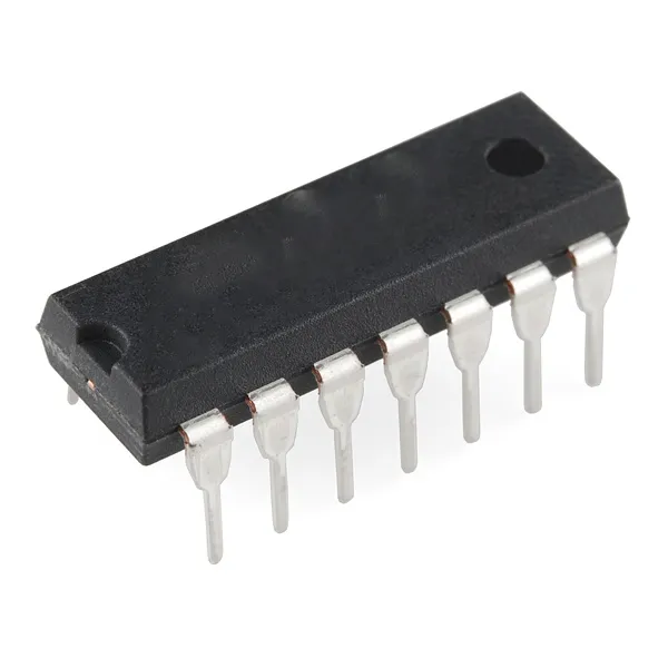
74HC74-7474 (Dual D-type flip-flop with set and reset-positive edge-trigger) is a high-quality electronic component designed for Arduino, prototyping, and educational electronics.
74LS74A flip-flop IC utilizes the Schottky TTL circuitry to produce high-speed D-type flip-flops. Each flip-flop has individual clear and set inputs, and also complementary Q and Q`(bar) outputs.
74LS74 Pinout Configuration
Pin Number
Pin Symbol
Name
Description
5,9
1Q / 2Q
Output
Output Pin of the Flip Flop
6,8
1Q’(bar) / 2Q’(bar)
Complementary Output
The inverted output pin of Flip Flop
3, 11
1CLK / 2CLK
Clock Input Pin
These pins must be provided with a clock pulse for the flip-flop
1,13
1CLR (bar) / 2CLR (bar)
Clear Data
Resets the flip-flop by clearing its memory
2,12
1D /2D
Data Input Pin
Input pin of the Flip Flop
4, 10
1PRE (bar) / 2PRE (bar)
PRE Input
Another Input pin for Flip Flop. Also referred to as a set pin
7
Vss
Ground
Connected to the ground of the system
14
Vdd/Vcc
Supply Voltage
Powers the IC typically with 5V
Features
Dual D Flip Flop Package IC
Operating Voltage: 2V to 15V
Propagation Delay: 40nS
Minimum High-Level Input Voltage: 2 V
Maximum Low-Level Input Voltage: 0.8V
Operating Temperature: 0 to 70°C
High-Level Output Current: 8mA
Available in 14-pin SO-14, SOT42 packages
Note: Complete Technical Details can be found in the 74LS74 datasheet given at the end of this page.
How to use 74LS74
Using a Flip-Flop is pretty straightforward. Simply power the IC using the Vcc and GND pin. As told earlier each flip-flop operates independently, just connect the input signals 2 and 3 for using the 1st flip-flop and you will get the output at pins 5 and 6. Pin 3 should be provided with a clock source normally a PWM signal from an MCU or 555 timers is used. The pin can be used to clear the data and reset the flip-flop by making it high. The complete working of the Flip flop can be understood by looking at the function table below. The symbol “X” indicates don’t care and the up-arrow indicates the rising edge of the signal.
INPUTS
OUTPUTS
PRE (bar)
CLR (bar)
CLK
D
Q
Q (bar)
L
H
X
X
H
L
H
L
X
X
L
H
L
L
X
X
H
H
H
H
H
H
L
H
H
L
L
H
H
H
L
X
Q 0
Q 0 (bar)
You can also simulate the IC to check if it would work as desired. Here I have used logic state and logic bits to view if the IC functions as it is supposed to, but you can replace them with the actual circuitry of your application to check if it would suit your needs. The gif file shown below can be verified with the truth table above to make sure that the IC works as desired.
Applications
Used as Shift Registers
Memory/Control Registers
Buffer Circuits
Sampling Circuits
Latching devices
Component Datasheet
74LS74 Datasheet It’s perfect for DIY makers, students, and anyone building custom electronic circuits or STEM kits.